


Home
Nanoscale Characterisation of Ferroelectric Materials: Scanning Probe Microscopy Approach
Barnes and Noble
Loading Inventory...
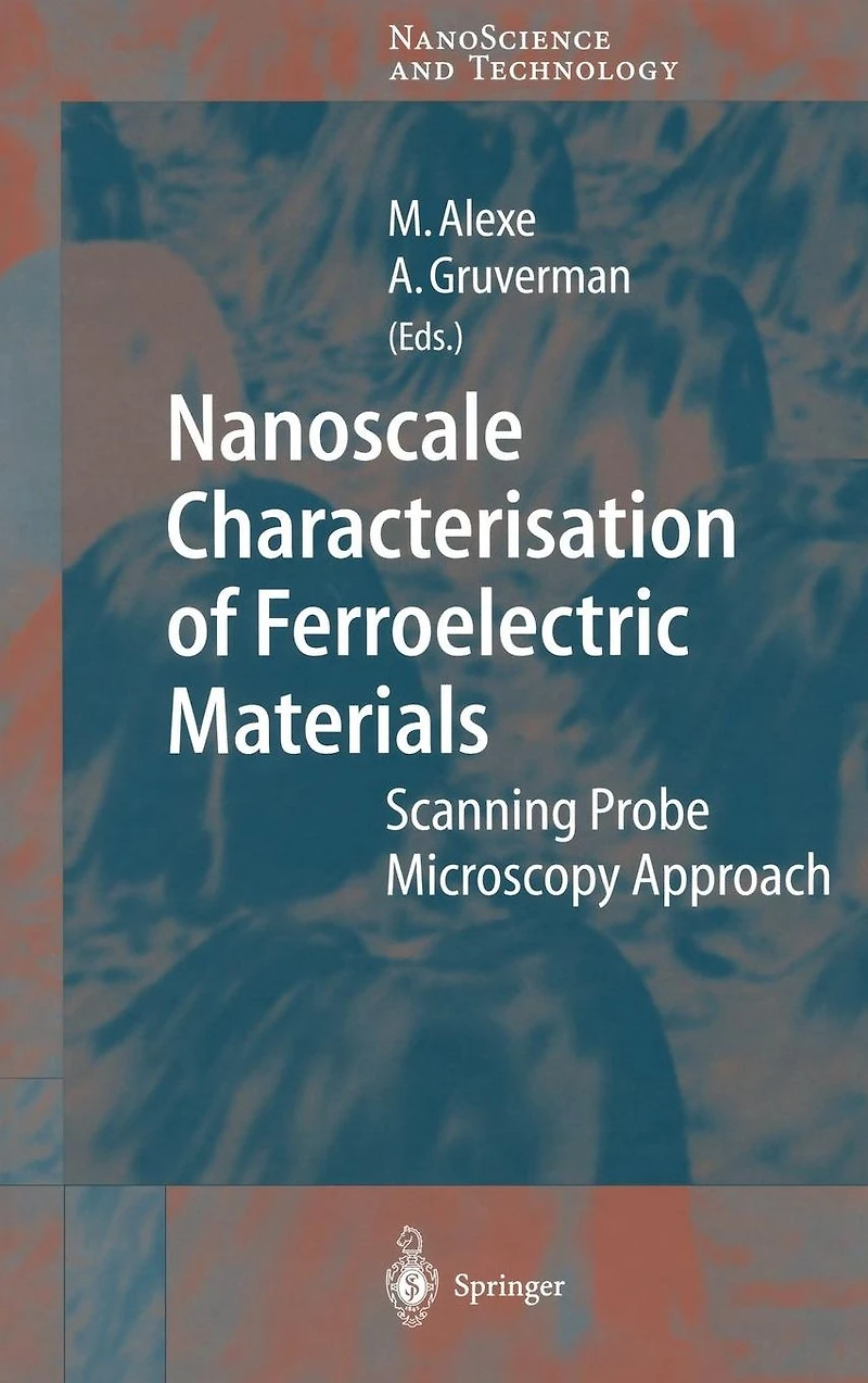
Nanoscale Characterisation of Ferroelectric Materials: Scanning Probe Microscopy Approach in Bloomington, MN
By Barnes & Noble
Current price: $169.99

Nanoscale Characterisation of Ferroelectric Materials: Scanning Probe Microscopy Approach in Bloomington, MN
Current price: $169.99
Loading Inventory...
Size: Hardcover
Among the main trends in our daily society is a drive for smaller, faster, cheaper, smarter computers with ever-increasing memories. To sustain this drive the computer industry is turning to nanotechnology as a source of new processes and func tional materials, which can be used in high-performance high-density electronic systems. Researchers and engineers have been focusing on ferroelectric materials for a long time due to their unique combination of physical properties. The ability of ferroelectrics to transform electromagnetic, thermal, and mechanical energy into electrical charge has been used in a number of electronic applications, most recently in nonvolatile computer memories. Classical monographs, such as Ferro electricity by E. Fatuzzo and W. J. Mertz, served as a comprehensive introduction into the field for several generations of scientists. However, to meet the challenges of the "nano-era", a solid knowledge of the ferroelectric properties at the nano scale needs to be acquired. While the science of ferroelectrics from micro-to lar ger scale is well established, the science of nanoscale ferroelectrics is still terra in cognita. The properties of materials at the nanoscale show strong size dependence, which makes it imperative to perform reliable characterization at this size range. One of the most promising approaches is based on the use of scanning probe microscopy (SPM) which has revolutionized materials research over the last dec ade.
Among the main trends in our daily society is a drive for smaller, faster, cheaper, smarter computers with ever-increasing memories. To sustain this drive the computer industry is turning to nanotechnology as a source of new processes and func tional materials, which can be used in high-performance high-density electronic systems. Researchers and engineers have been focusing on ferroelectric materials for a long time due to their unique combination of physical properties. The ability of ferroelectrics to transform electromagnetic, thermal, and mechanical energy into electrical charge has been used in a number of electronic applications, most recently in nonvolatile computer memories. Classical monographs, such as Ferro electricity by E. Fatuzzo and W. J. Mertz, served as a comprehensive introduction into the field for several generations of scientists. However, to meet the challenges of the "nano-era", a solid knowledge of the ferroelectric properties at the nano scale needs to be acquired. While the science of ferroelectrics from micro-to lar ger scale is well established, the science of nanoscale ferroelectrics is still terra in cognita. The properties of materials at the nanoscale show strong size dependence, which makes it imperative to perform reliable characterization at this size range. One of the most promising approaches is based on the use of scanning probe microscopy (SPM) which has revolutionized materials research over the last dec ade.









Find at Mall of America® in Bloomington, MN
Visit at Mall of America® in Bloomington, MN