Home
Nanolithography: A Borderland between STM, EB, IB
Barnes and Noble
Loading Inventory...
Nanolithography: A Borderland between STM, EB, IB in Bloomington, MN
Current price: $219.99

Nanolithography: A Borderland between STM, EB, IB in Bloomington, MN
Current price: $219.99
Loading Inventory...
Size: OS
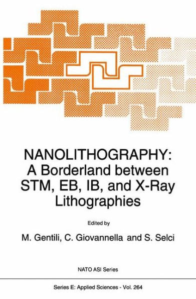
Success in the fabrication of structures at the nanometer length scale has opened up a new horizon to condensed matter physics: the study of quantum phenomena in confined boxes, wires, rings, etc. A new class of electronic devices based on this physics has been proposed, with the promise of a new functionality for ultrafast and/or ultradense electronic circuits. Such applications demand highly sophisticated fabrication techniques, the crucial one being lithography. Nanolithography contains updated reviews by major experts on the well established techniques electron beam lithography (EBL), X-ray lithography (XRL), ion beam lithography (IBL) as well as on emergent techniques, such as scanning tunnelling lithography (STL).
Success in the fabrication of structures at the nanometer length scale has opened up a new horizon to condensed matter physics: the study of quantum phenomena in confined boxes, wires, rings, etc. A new class of electronic devices based on this physics has been proposed, with the promise of a new functionality for ultrafast and/or ultradense electronic circuits. Such applications demand highly sophisticated fabrication techniques, the crucial one being lithography. Nanolithography contains updated reviews by major experts on the well established techniques electron beam lithography (EBL), X-ray lithography (XRL), ion beam lithography (IBL) as well as on emergent techniques, such as scanning tunnelling lithography (STL).
